
IC Fabrication Startup Equity Stake For Sale in Kolkata, India
Pre-revenue semiconductor manufacturer seeking co-founder with investment 20L-5Cr for wafer fabrication, compound semiconductors/ATMP/ASIC services.
Premium Plan
| Established | 0-1 year(s) |
| Employees | 50 - 100 |
| Legal Entity | Public Limited Company |
| Reported Sales | Nil |
| Run Rate Sales | Nil |
| EBITDA Margin | Nil |
| Industries | IC Fabrication + 1 more |
| Locations | Kolkata |
| Local Time | 12:26 PM Asia / Kolkata |
| Listed By | Business Owner / Director |
| Status | Active |
Partial Stake Sale
USD
20 thousand
for
5.0%
stake
(Native Currency: USD 20,000)
Reason: Seeking funding to commence immediate construction of the facility, with operations scheduled to beg...
View More
Interested in connecting with advisors
Name, Phone, Email
Available after connect
Business Name
Available after connect
User Verification
Documents


Business Overview
- Pre-revenue semiconductor technology company developing a large-scale semiconductor manufacturing and technology platform in India.
- The company is targeting automotive, telecommunications, healthcare, aerospace, energy, and IoT sectors.
- The planned pure-play wafer fabrication business will focus on 28nm–65nm CMOS logic and analog/mixed-signal ICs.
- The planned compound semiconductor fab will focus on III-V technologies, including GaAs and InP RF chips, along with MEMS sensor fabrication.
- ATMP and backend capabilities are planned to include high-speed SMT assembly, wafer dicing, multi-zone reflow packaging, and 3D AOI/AXI testing.
- ASIC and design services will cover RTL-to-GDS custom silicon design for automotive, aerospace, and IoT OEMs.
- The business model is based on a B2B "Pure-Play Foundry" and "Wafer-as-a-Service" model.
- The company aims to generate predictable cash flows through long-term captive offtake agreements for 28nm logic and compound/MEMS chips.
- The leadership team brings decades of combined global experience in deep-tech scaling, semiconductor supply chain management, and execution of large industrial capital projects.
- The company has an anchor relationship with global companies and is cultivating an advanced sales pipeline of 15+ global OEMs across automotive, telecommunications, and consumer electronics.
- The company is in the final stages of establishing joint ventures and technology-transfer licensing agreements with top-tier global foundries across Taiwan, Israel, and the United States.
- The company's strategic blueprint has received recognition from industry consortiums and national media as a pioneering industrial initiative aimed at supporting Eastern India's technology ecosystem and the government's Aatmanirbhar Bharat mandate.
- The company is seeking investment to develop and scale its semiconductor manufacturing, backend, and design capabilities.
- Currently registered as a public limited company with the MCA and holding a valid company PAN. Statutory licenses will be acquired at the time of commencing operations.
- The company is targeting automotive, telecommunications, healthcare, aerospace, energy, and IoT sectors.
- The planned pure-play wafer fabrication business will focus on 28nm–65nm CMOS logic and analog/mixed-signal ICs.
- The planned compound semiconductor fab will focus on III-V technologies, including GaAs and InP RF chips, along with MEMS sensor fabrication.
- ATMP and backend capabilities are planned to include high-speed SMT assembly, wafer dicing, multi-zone reflow packaging, and 3D AOI/AXI testing.
- ASIC and design services will cover RTL-to-GDS custom silicon design for automotive, aerospace, and IoT OEMs.
- The business model is based on a B2B "Pure-Play Foundry" and "Wafer-as-a-Service" model.
- The company aims to generate predictable cash flows through long-term captive offtake agreements for 28nm logic and compound/MEMS chips.
- The leadership team brings decades of combined global experience in deep-tech scaling, semiconductor supply chain management, and execution of large industrial capital projects.
- The company has an anchor relationship with global companies and is cultivating an advanced sales pipeline of 15+ global OEMs across automotive, telecommunications, and consumer electronics.
- The company is in the final stages of establishing joint ventures and technology-transfer licensing agreements with top-tier global foundries across Taiwan, Israel, and the United States.
- The company's strategic blueprint has received recognition from industry consortiums and national media as a pioneering industrial initiative aimed at supporting Eastern India's technology ecosystem and the government's Aatmanirbhar Bharat mandate.
- The company is seeking investment to develop and scale its semiconductor manufacturing, backend, and design capabilities.
- Currently registered as a public limited company with the MCA and holding a valid company PAN. Statutory licenses will be acquired at the time of commencing operations.
Products & Services Overview
- Pure-play wafer fabrication: 28nm–65nm CMOS Logic & analog/mixed-signal ICs.- Compound semiconductor Fab: III-V (GaAs, InP) RF chips and MEMS sensor fabrication.
- ATMP/backend Services: High-speed SMT assembly, wafer dicing, multi-zone reflow packaging, and 3D AOI/AXI testing.
- ASIC & design services: RTL-to-GDS custom silicon design for automotive, aerospace, and IoT OEMs.
Will cater to automotive, telecom, healthcare, aerospace, energy, IoT, and consumer electronics OEMs.
Assets Overview
Assets:Machinery and equipment valued at approximately INR 43,000 crores (USD 4.556 billion), with an advance of INR 133 crores (USD 14 million) already paid.
Facilities Overview
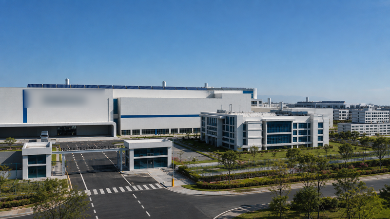
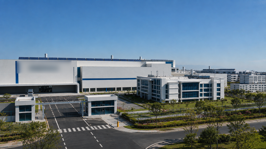
Planned facility overview.1. Site overview & built-up area.
The Facility is designed as a state-of-the-art, high-capacity, and highly secure industrial complex.
Total land area: 55 Acres of contiguous, vibration-isolated land.
Location: Bengal Silicon Valley Tech Hub, New Town, Kolkata, West Bengal.
Built-up area allocation: The 55-acre campus will be zoned into highly segregated modules to prevent cross-contamination, ensuring absolute isolation between silicon logic processes, compound/exotic materials processing, and backend packaging, along with dedicated utility staging areas (substations, water plants)
2. Rental & lease arrangements.
Lease Structure: The 55-acre parcel is being negotiated under an expedited 99-year long-term industrial lease agreement with the West Bengal Housing Infrastructure Development Corporation (WBHIDCO).
Status: Advanced allocation discussions are currently underway, requesting "Ultra-Mega Project Status" to secure deep structural discounts on the lease premium, waivers on stamp duty, and long-term utility tariff subsidies.
3. Architectural structure & number of floors.
Semiconductor fabs operate on complex vertical architectures to ensure continuous, sterile laminar airflow and strict vibration control, unlike standard commercial manufacturing, of which the construction is under process at the foundation level and will be completed in coming 2 years.
Building 1: 28nm Silicon Foundry (ISO Class 2 & 3)
Designed as a "Ballroom-style" vertical mega-fab, built on vibration-cancelling "Waffle Slabs" to isolate lithography tools from micro-seismic activity.
Level 3 (Top Floor - Air Plenum): 100% dedicated to HVAC and air circulation. Houses massive Make-up Air Units (MAUs) that push temperature-and-humidity-controlled air down through Ultra-Low Penetration Air (ULPA) ceiling grids.
Level 2 (middle floor - main cleanroom): The primary production floor divided into isolated bays (Lithography, Etch, Deposition, Metrology). Wafers are transported via ceiling-mounted Automated Overhead Hoist Transports (OHTs).
Level 1 (ground floor/basement - sub-fab): The mechanical "engine room" directly beneath the cleanroom. Houses roughing vacuum pumps, point-of-use toxic gas scrubbers, and Teflon-coated bulk chemical delivery pipes.
Building 2: Compound semiconductor & MEMS Fab (ISO Class 4 & 5)
Physically isolated to prevent cross-contamination from exotic III-V materials.
Level 2 (Cleanroom floor): Houses Epitaxy Growth (MOCVD/MBE), Deep Reactive Ion Etching (DRIE) for MEMS cavities, Wafer Bonding, and Noble Metal wet benches.
Level 1 (Sub-Fab Level): Dedicated to specialized hazardous waste sorting and localized effluent treatment tanks (e. g. , handling Arsenic or Phosphine residues).
Building 3: ATMP / SMT Backend Assembly.
Ground floor (horizontal flow): A sprawling, linear, ground-floor operation designed for high-speed continuous flow. It features 6 primary zones moving from Incoming Quality Control (IQC) to Solder Paste Printing, High-Speed Pick & Place, Multi-Zone Nitrogen Reflow, 3D AOI/AXI Inspection, and final Testing.
Zone E: Administration, security & R&D gateway.
Ground floor: High-security biometric checkpoint and the main "Gowning Air-locks" equipped with high-velocity air showers.
First floor: Executive C-Suite, R&D/Failure Analysis Labs (equipped with Electron Microscopes), and the MAKAUT/Jadavpur University joint training centre featuring a dummy cleanroom.
4. Plant & Machinery (P&M) details.
The total Stage 1 Capex for P&M and Utility Machinery is strategically optimized using a blend of advanced new tooling and highly reliable, refurbished platforms (such as ASML PAS 5500 / Twinscan systems).
A. Core Wafer Fabrication Equipment (28nm & Mature Nodes).
Lithography scanners: ASML ArF Immersion Scanners (for critical 28nm HKMG resolution) and ASML KrF / i-line Scanners (for non-critical layers).
Deposition & etch: Atomic Layer Deposition (ALD) chambers, CVD/PVD tools, and Plasma Etchers (ICP/CCP RIE) for precise vertical channel etching.
Doping & planarization: High/Medium Current Ion Implanters, Rapid Thermal Processing (RTP) furnaces, and Chemical Mechanical Polishing (CMP) tracks.
Metrology: CD-SEM (Critical Dimension Scanning Electron Microscopes) and Optical defect scanners.
B. Compound & MEMS tooling.
Epitaxy reactors: MOCVD / MBE systems for growing specialized crystalline layers (GaAs, InP).
Specialized Etch/bonding: Deep RIE (DRIE) etchers for MEMS, Anodic/Fusion Wafer Bonders, and E-Beam Evaporators for noble metals (Gold/Platinum).
C. ATMP, automation, & packaging machinery.
Automation: Factory-wide AMHS (Automated Material Handling Systems) featuring continuous overhead rails, FOUPs, and robotic hoists managed by centralized CIM/MES software.
Packaging line: Precision Wafer Dicing Saws, Ultrasonic Wire Bonders, High-Speed Pick & Place SMT Robots, multi-zone Nitrogen Reflow Ovens, and 3D Automated X-Ray Inspection (AXI).
D. Facility & utility machinery backbone.
Power reliability: 220kV/400kV Gas Insulated Switchgear Substation supported by a massive Diesel Rotary UPS (DRUPS) kinetic flywheel farm to prevent voltage sags.
Water & waste: 18 MΩ Ultra-Pure Water (UPW) Generation Plant capable of filtering 8 to 10 MGD, and an industrial Effluent Treatment Plant (ETP) with point-of-use toxic gas abatement systems.
Capitalization Overview
Ownership: 3 directors and 7 shareholders, with promoter holding majority stake.The company is debt‑free with no outstanding loans.
The facility: comprehensive financial report.
1. Executive financial summary & project cost.
The Company's facility project represents a phased economic juggernaut, aggressively scaled to capture the booming global and domestic semiconductor market. The capital deployment is structured across two primary expansion stages:
Stage 1 (Launch): Total estimated gross CapEx: USD 7.0 billion.
Target production capacity: 70,000 Wafer Starts Per Month (WSPM).
Scope: Establishment of the 28nm Silicon Foundry, Compound/MEMS Fab, and PCBA/SMT Backend.
Stage 2 (Expansion in 4 years): cumulative gross CapEx: USD 14 billion.
Target production capacity: 130,000 WSPM.
(Note: Net Corporate Capital Expenditure for Stage 1 is effectively modeled between USD 3.5 billion and USD 5 billion upon the realization of aggressive government subsidies).
2. Capital Expenditure (CapEx) breakdown.
Building a mega-fab requires immense upfront capital, categorized broadly into highly specialized civil infrastructure and precision fabrication equipment.
A. Facilities & cleanroom infrastructure.
Semiconductor construction costs heavily outweigh standard commercial real estate due to the necessity for absolute vibration isolation and extreme air filtration.
Site development & core shell (USD 150M – USD 250M): Land acquisition, deep concrete waffle slabs, micro-seismic vibration isolation, and heavy steel frameworks.
Cleanroom Buildout (USD 100M – USD 150M): ISO Class 3/4 to 7/8 cleanroom setups, raised perforated floors, specialized HVAC, ULPA/HEPA filtration grids, and anti-static wall panelling.
Sub-fab utilities (USD 80M –USD 120M): 18 MΩ Ultra-Pure Water (UPW) plants, point-of-use toxic gas abatement systems, and on-site nitrogen generators.
Facilities subtotal: USD 330M – USD 520M.
B. Silicon fab equipment (Building 1)
Precision lithography and high-vacuum processing tools dominate the equipment budget. The company optimizes this by utilizing a strategic mix of new and highly cost-effective refurbished systems (e. g, ASML PAS 5500s).
Lithography (ArF & KrF): USD 300M – USD 450M (Refurbished ArF dry scanners for 45nm/65nm and KrF step-and-scan systems for mature layers).
Deposition (CVD, PVD, ALD): USD 200M+.
Remaining equipment Capex spans plasma etchers, ion implanters, CMP tracks, and automated material handling systems (AMHS/OHTs).
3. Operating Expenditure (OpEx) Analysis.
In the first year of operations, the operating costs for the semiconductor manufacturing plant will be significant. By the fifth year, total operational costs will increase substantially in absolute terms as production volumes scale and capacity utilization reaches its peak.
Standard OpEx distribution:
Raw material cost (40% – 45%): The largest operational driver, encompassing blank silicon wafers, photomasks, highly specialized chemicals (acids, slurries), photoresists, and specialty electronic gases.
Utility cost (25% – 30%): Massive continuous power consumption (supported by the DRUPS farm) and heavy industrial water intake.
Other expenses: Salaries and Wages (for highly skilled cleanroom technicians and engineers), Depreciation on heavy equipment, Maintenance & Repairs, Packaging, Transportation, and Taxes.
4. Subsidies & funding structure.
The financial viability and rapid ROI of the company's project are heavily anchored in its alignment with aggressive sovereign manufacturing initiatives.
Central Government (India Semiconductor Mission - ISM): The project relies on the Modified ISM Scheme, which guarantees a flat 50% pari-passu (equal footing) Capex subsidy for approved Silicon CMOS fabs, Compound Semiconductor facilities, and ATMP/OSAT units. This effectively halves the corporate financial burden.
State Government (West Bengal): The company is actively negotiating "Ultra-Mega Project Status" with the Government of West Bengal. This status unlocks further critical financial levers, including massive capital subsidies, long-term electricity duty waivers, stamp duty exemptions, and deep structural discounts on the 99-year WBHIDCO land lease.
5. Profitability & margin projections.
By targeting the "sweet spot" of mature and 28nm nodes alongside specialized Compound MEMS—and drastically lowering depreciation burdens via 50% ISM subsidies and refurbished lithography tools—the facility is engineered for rapid, high-margin returns.
Estimated gross margin: 50% – 60% (Supported by stable, long-term captive demand from automotive, agricultural, and IoT sectors).
Estimated net profit margin: 20% – 30%
(Disclaimer: Financial projections are strategic models based on industry averages, current PLI/ISM frameworks, and target WSPM capacity. Actual expenditures and income will vary based on final supply chain negotiations, market fluctuations, and finalized government MoUs).
Recent Activity
-
1 day agoDirector, IT, Digital Media, CE, Mumbai, Individual Investor / Buyer connected with the Business
-
2 weeks, 1 day agoCo-Founder, IT Services, Mergers And Acquisitions, Head Hunting, Pune, Corporate Investor / Buyer connected with the Business
-
2 weeks, 1 day agoDirector, Mumbai, M&A Advisor connected with the Business
Tags:
IC Fabrication Startup Investment Opportunity in Kolkata, India
·Semiconductors Startup Investment Opportunity in Kolkata, India
·IC Fabrication Startup Equity Stake For Sale in Kolkata, India
·Semiconductors Startup Equity Stake For Sale in Kolkata, India
·IC Fabrication Startup Investment Opportunity in Calcutta
·Semiconductors Startup Investment Opportunity in Calcutta
·IC Fabrication Startup Equity Stake For Sale in Calcutta
·Semiconductors Startup Equity Stake For Sale in Calcutta
·Invest in IC Fabrication Startup in Kolkata, India
·Invest in Semiconductors Startup in Kolkata, India
·IC Fabrication Startup Investment Opportunity
·Semiconductors Startup Investment Opportunity
·Invest in IC Fabrication Startup in Calcutta
·Invest in Semiconductors Startup in Calcutta
·Investment Opportunity in Kolkata, India
·Investment Opportunity in Calcutta
·Invest in IC Fabrication Startup
·Invest in Semiconductors Startup
·Invest in Kolkata, India
·Invest in Calcutta
Disclaimer: SMERGERS is a regulated marketplace for connecting business sell sides with investors, buyers, lenders and advisors. Neither SMERGERS represents nor guarantees that the information mentioned above is complete or correct. Note that SMERGERS is not liable for any loss, damage, costs, claims and expenses whatsoever arising from transacting with any other user from the website. The final responsibility of conducting a thorough due diligence and taking the transaction forward lies with the users. Please read best practices on SMERGERS.
Contact Business
 1 Investor contacted this Business this week.
Register below to connect now!
1 Investor contacted this Business this week.
Register below to connect now!
- Social
- Register
- Login
Who uses SMERGERS?



... and 72,000+ other businesses of all sizes.
Disclaimer: SMERGERS is a regulated marketplace for connecting business sell sides with investors, buyers, lenders and advisors. Neither SMERGERS represents nor guarantees that the information mentioned above is complete or correct.
You might also be interested in these businesses